Selected Area Deposition of PtCx Nanostructures: Implications for functional coatings of 3D Nanoarchitectures
Researchers from the University of Tennessee and Oak Ridge National Lab used the Waviks' Vesta to explore pyrolytic laser chemical vapor deposition processes on 3D PtC composite nanostructures. Their work was published in ACS Applied Nano Materials. Their results indicate the ability to initiate the deposition process on sub-diffraction-limit nanoscale features.

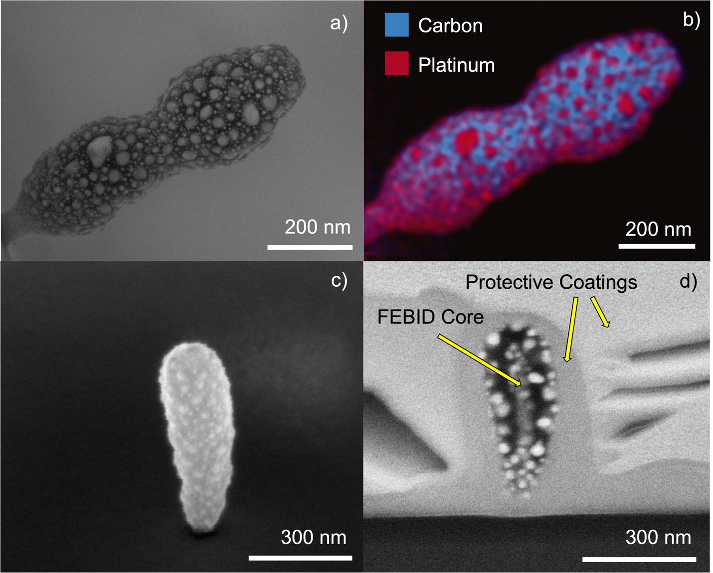
a) SEM image and b) EDS map of a of nanopillar after selected area laser processing. EDS maps of the pillar showing platinum-rich regions embedded in a C matrix indicating phase separation and Pt grain growth during the laser processing. c) SEM image of an as laser grown pillar and the associated backscatter SEM image of a FIB cross-section showing the phase separation where Pt are the bright regions. The light, top amorphous material is a focused ion beam induced deposition protective layer for cross-sectioning, and the darker amorphous layer under that is initial FEBID protective deposition. The EBID as-deposited nanostructures were grown using a single pixel dwell at 5kV, 98 pA. 75nm beam diameter by defocusing, for 40s (a,b) and 30s (c,d) Laser CVD was accomplished using 4.8W, 10 s 915 nm pulses at 1kHz for 60 s.
The teams from Oak Ridge National Lab and the University of Tennessee demonstrated that controlling the thermal transport in nanomaterial architectures could be a useful means to spatially controlled localized photothermally stimulated chemical reactions and induce selected area reactions.
Reference:
Exploring the composition, phase separation and structure of AgFe alloys for magneto-optical applications,
Materials Science and Engineering: B,
Volume 266,
2021,
115044,
ISSN 0921-5107,
https://doi.org/10.1016/j.mseb.2021.115044.
