3D nanoprinting via laser-assisted electron beam induced deposition
Teams from University of Tennessee, Graz Centre for Electron Microscopy, and Oak Ridge National Lab explored 3D nanoprinting via laser-assisted electron beam induced deposition. Their work was published in the Beilstein Journal of Nanotechnology.

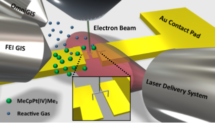
Figure 1: Schematic illustrating the experimental system which includes a laser delivery system, precursor and co-reactant gas delivery systems, and the electron beam all coincident to the same region. The schematic also illustrates the deposition of the 3D suspended bridge structures grown for the electrical measurements.
The first fully incorporated 3D transistor logic was reported in 2012. Further 3D device concepts and architectures will require the development of new 3D nanoscale fabrication techniques which will inevitably enhance performance and add functionality to nanoscale devices. Emerging applications include, but are not limited to, high strength nanolattices, optical metamaterials, accurate molecular detection [4], the study of biological systems important in determining cancer treatment options, and reliable, low cost, high performance magnetic hard disk drives. A variety of fabrication techniques have been used to construct multi-dimensional nanostructures with differing degrees of success. The Waviks Vesta can be used to purify these deposits by removing excess precursor materials.
Reference:
Lewis, B. B.; Winkler, R.; Sang, X.; Pudasaini, P. R.; Stanford, M. G.; Plank, H.; Unocic, R. R.; Fowlkes, J. D.; Rack, P. D. Beilstein J. Nanotechnol. 2017, 8, 801–812.
doi:10.3762/bjnano.8.83
