Laser Assisted Focused Helium Ion Beam Induced Etching Both With and Without Xenon-Difluoride Gas Assist
Researchers from University of Tennessee, Intel Corporation, Oak Ridge National Lab and Waviks explored laser assisted focused Helium Ion Beam induced etching both with and without xenon-difluoride gas assist. Their work was published in ACS Applied Materials & Interfaces.

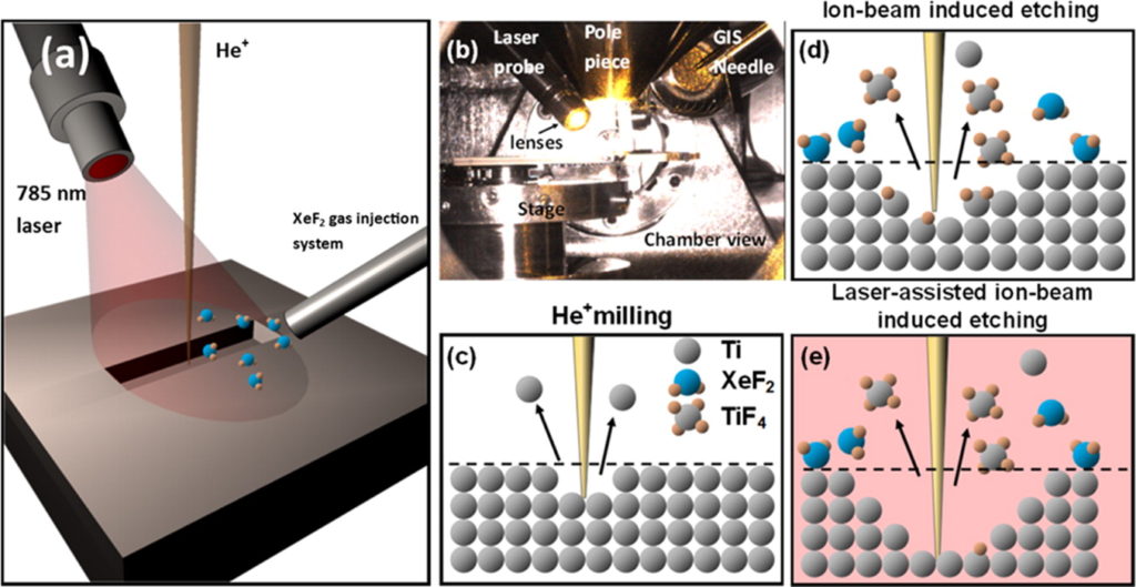
Figure 1. (a) Schematic of the focused ion beam induced etching (FIBIE) setup. The focused 785 nm laser beam, focused He+ beam, and gas injection nozzle share a common confocal point on the Ti film surface. (b) In-chamber digital photograph of the experimental setup with the beam, laser probe, and gas sources indicated. The GIS needle is retracted in this image. (c) Schematic of a He+ milling process of Ti. (d) Schematic of a FIBIE process with the XeF2 chemical assist. (e) Schematic of a laser-assisted FIBIE process.
Focused helium ions have been used for nanoscale synthesis in a variety of applications in recent years and offer an enhanced resolution relative to the standard liquid Ga ion source. This has resulted in synthesis of nanostructures with sub-10 nm resolution via deposition, etching, and lithography. However, due to low sputter yields of He+, patterning by material removal requires high doses, which results in the formation of undesired subsurface damage and He bubbling. This is undesirable for many applications and limits the effectiveness of focused He+ as a nanofabrication candidate. Therefore, for robust nanoscale synthesis with the helium ion microscope (HIM), processes should be developed which mitigate subsurface damage as well as minimize the He+ dose required for processing. The Waviks Vesta proved to be successful in minimizing subsurface damage and bubbling and reduced the required dose for etching.
Reference:
DOI: 10.1021/acsami.6b09758
