Electron Beam Induced Deposition Purification via Pulsed Laser Induced Oxidation Reaction
Teams from Oak Ridge National Laboratory, University of Tennessee, Utah State University, and Graz University of Technology demonstrated electron beam induced deposition purification via pulsed laser induced oxidation reaction using the Waviks Vesta. Their work was published in ACS Applied Materials & Interfaces.

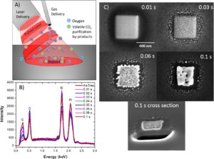
Figure 1. (A) Schematic of the laser annealing setup with approximately 100 μm laser spot size under O2 flow. (B) EDS measurements of a ∼140-nm-thick PtC5 EBID deposit annealed with 100 μs pulses at 0.1% duty cycle as a function of the exposure times. (C) Images of laser-annealed patterns at different exposure times. The deposit annealed for 0.1 s exposure time was also cross-sectioned and is pictured here.
Electron-beam-induced deposition (EBID) is a synthesis technique that is dictated by a focused electron beam and stimulates a localized reaction of precursor species. The result is a nanoscale synthesis technique that can conveniently grow materials “on-demand” via a prescribed electron-beam raster sequence. Significant advances have been made by elucidating the critical electron–precursor–solid interactions that occur in the EBID process, which has enabled better control and higher resolution. Thus, several applications have emerged for nanostructured materials grown via EBID, such as specialized scanning probe tips, nanomagnetic logic and devices, nanophotonics, field-emission emitters, new sensor concepts exploiting nanogranular behavior, maskless lithography, lithography mask editing, superconducting nanostructures, and electrical contacts on-demand to name a few. The Vesta can purify EBID deposits and thus give you bulk metallic properties at the nanoscale.
Reference:
DOI: 10.1021/am506246z
