High-resolution laser-induced graphene. Flexible electronics beyond the visible limit
Researchers from the University of Tennessee, Oak Ridge National Lab, and Rice University used the Waviks' Vesta to fabricate high resolution graphene in-situ. Their work was published in ACS Applied Materials and Interfaces.

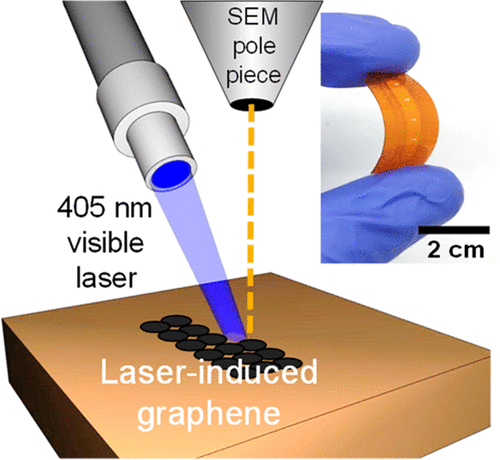
Schematic of experimental setup that uses a 405 nm laser mounted on high-angle port of SEM. Laser Induced Graphene (LIG) is formed in situ in the SEM chamber. Flexible electronic fabricated using LIG.
The researchers were able to achieve a >60% reduction in LIG feature size by using hte Waviks Vesta coupled to a 405nm laser. This reduction can enable direct write formation of flexible electronics in situ.
Reference:
High-Resolution Laser-Induced Graphene. Flexible Electronics beyond the Visible Limit
Michael G. Stanford, Cheng Zhang, Jason D. Fowlkes, Anna Hoffman, Ilia N. Ivanov, Philip D. Rack, and James M. Tour
ACS Applied Materials & Interfaces 2020 12 (9), 10902-10907
DOI: 10.1021/acsami.0c01377
