Vesta for TEM
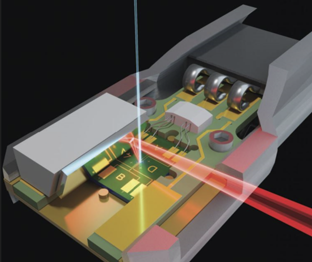
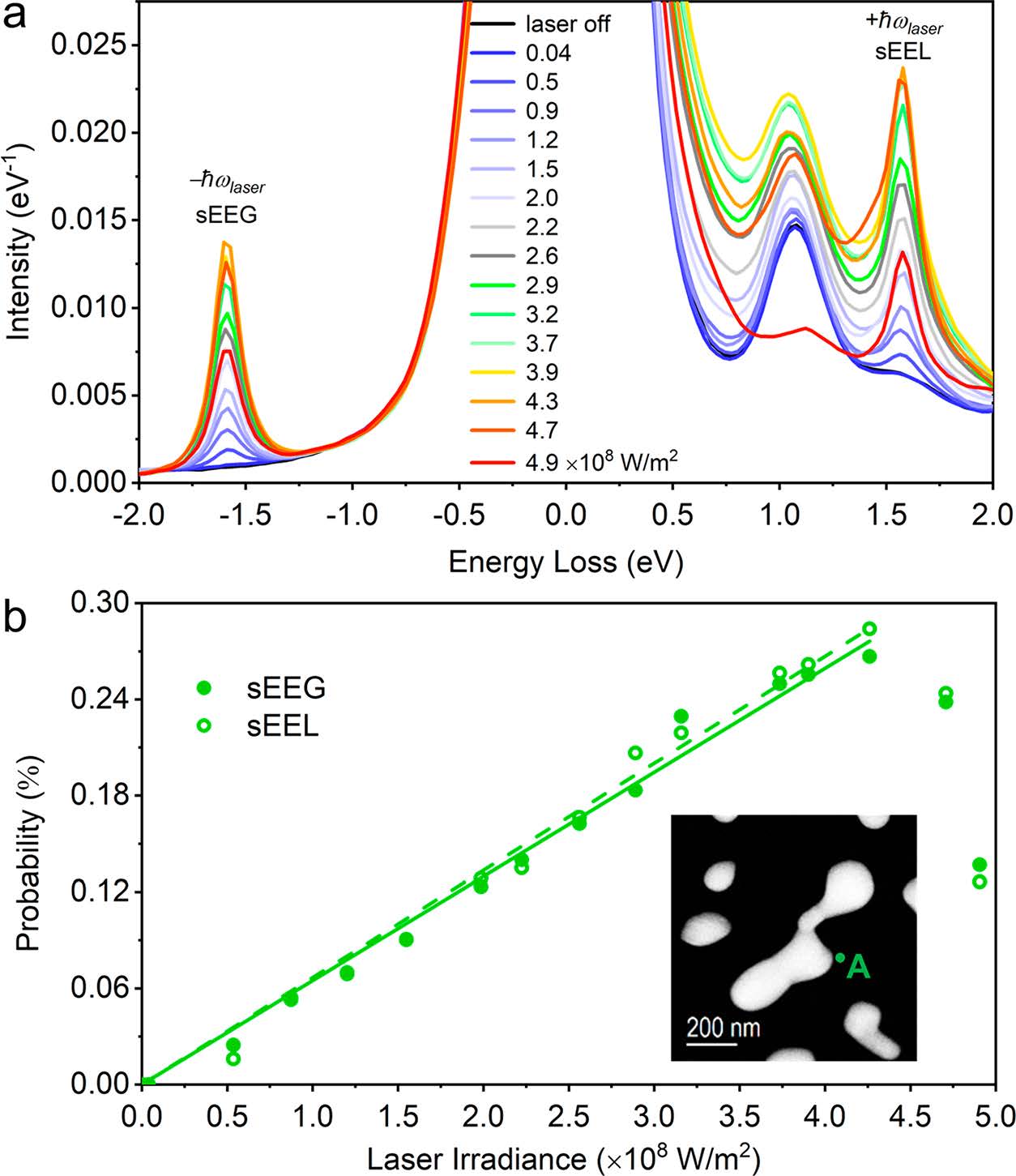
The Vesta for TEM provides precise Local heating and excitation of a specific area on the TEM sample with a spot size of under 10 µm diameter. Waviks’ Vesta™ has no inherent high temperature limit, meaning the irradiated region on the sample can be safely and deliberately heated to evaporation/sublimation with minimal thermal-mechanical drift during heating. This capability gives the user the ability to rapidly and repeatedly ramp the sample temperature up and down independent of the sample holder temperature. The laser can be used in continuous mode or pulsed with a <10 ns rise time. This gives the user the convenience of conducting multiple experiments in one session on a single sample using different pristine spots on that same sample. No expensive one-time-use sample holders or coupons required. The Vesta can encompass wavelengths from the UV to the IR and laser energies from 1mW to 25W.
The Vesta™ system includes the Waviks Compact Nanomanipulator which enables 3 axis programmable translation of the laser probe with saved locations for the focus of each laser wavelength. The software is designed for convenient routine use. The Vesta™ can be automated from a remote location via an Ethernet link, and the software includes a Python SDK for easy remote automation.
OPTIONS AND APPLICATIONS:
Vesta for FIB/SEM/Tabletop SEM
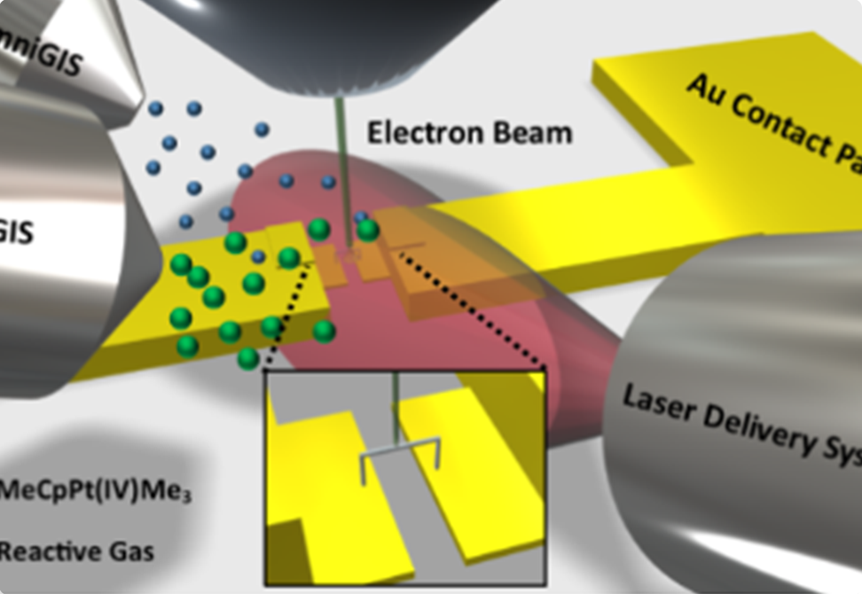
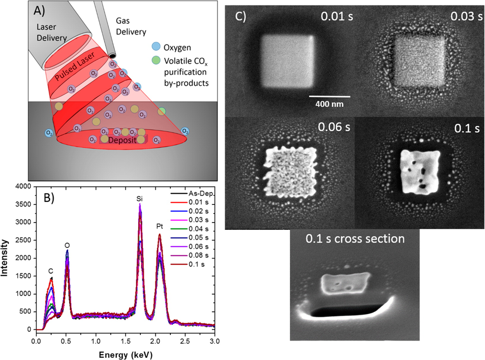
The Vesta for FIB/SEM provides the same benefits as the Vesta for TEM as well as additional spectroscopy applications including Raman, Cathodoluminescence, and Photoluminescence. Users have the ability to conduct in situ local thermal annealing as well as purification of electron beam induced deposits. The Vesta for FIB/SEM works especially well with our high powered laser options for heating bulk materials. This system also includes large field of view imaging so users can see the laser spot on the sample for easy alignment.
OPTIONS AND APPLICATIONS:
Electron Beam Induced Current
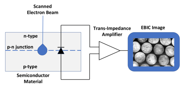
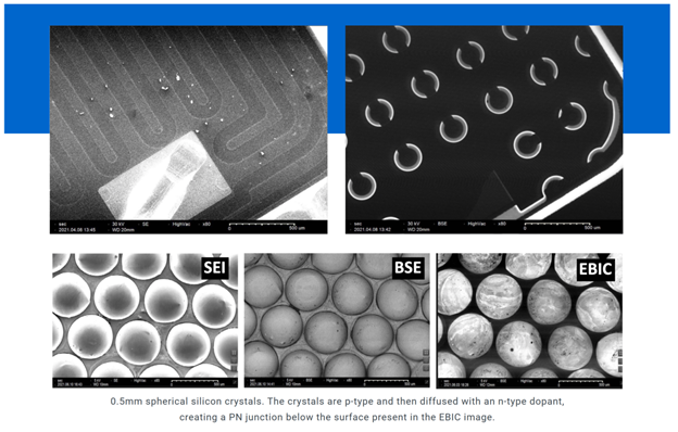
Electron Beam Induced Current (EBIC) imaging is a method performed in the SEM that reveals electrically active structures and defects in a semiconductor sample that contains a p-n junction or Schottky diode. The internal field in the junction region separates electron-hole pairs generated by the electron beam and collects the current produced. This EBIC signal is amplified by a current-sensitive trans-Impedance amplifier and enables a real-time EBIC image of the junction region. Waviks’ EBIC imaging accessory uses a rechargeable battery, double-shielded connections, a custom SEM electrical feedthrough and dedicated sample holders for ultra-quiet detection of the EBIC current signal.
READY TO GET STARTED? CONTACT US TODAY!
