
In situ Raman spectroscopy
Acquire vibrational spectra from regions of interest while preserving experiment context inside the target instrument.
Raman measurement path
Measure Raman signatures from the electron-beam coincident point on a tabletop SEM, full-size SEM, or full-size FIB/SEM system.
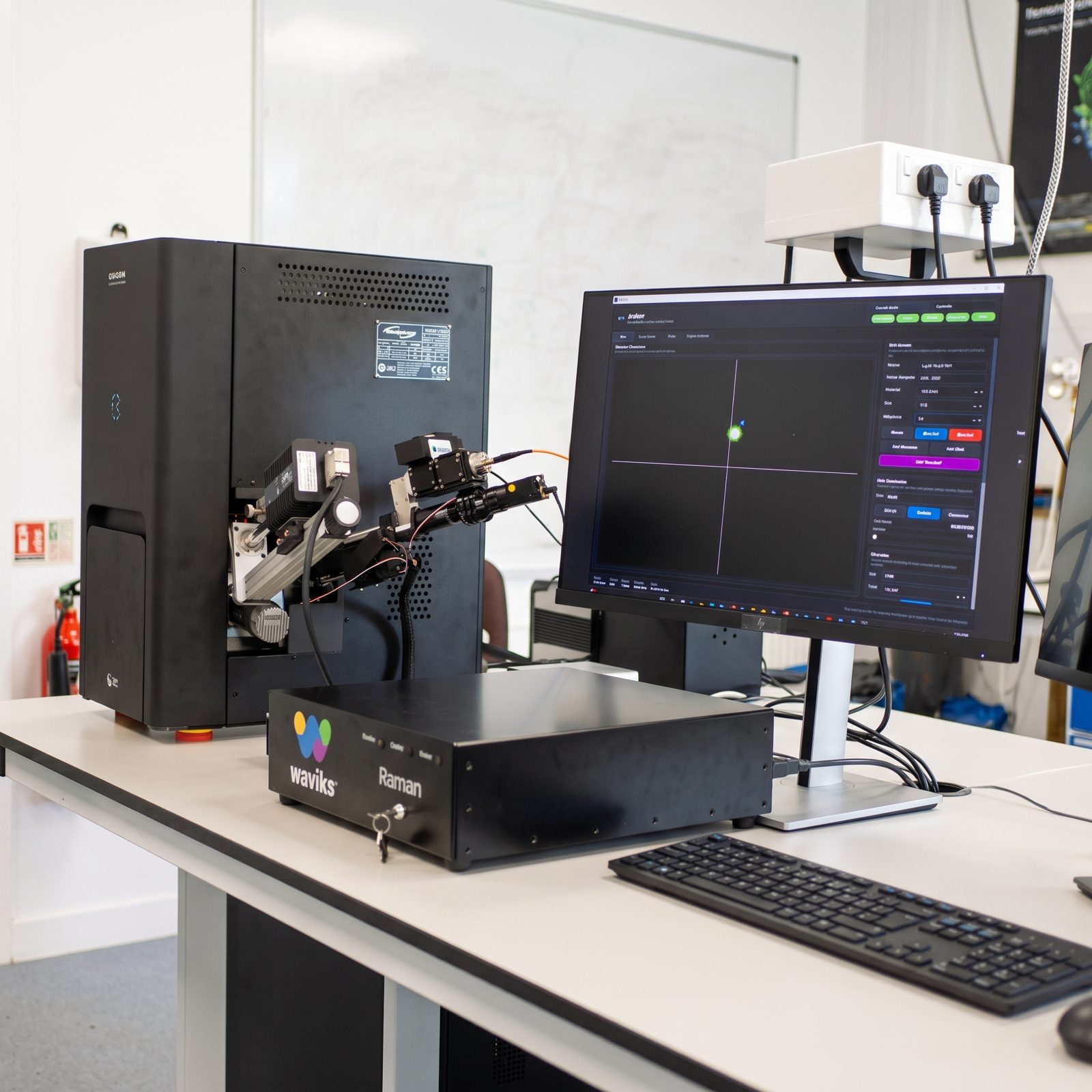
Measurement overview
Waviks Raman systems combine laser delivery, collection optics, spectrometer connection, alignment tools, and Aether acquisition. Options include tabletop SEM and full-size SEM/FIB installations, as well as standalone Raman. Optical excitation in TEM requires a separate review of the installed geometry.
Capabilities
Technical review confirms microscope access, Raman wavelength, fiber-coupled spectrometer fit, collection geometry, sample fluorescence risk, and experiment goals.
Acquire vibrational spectra from regions of interest while preserving experiment context inside the target instrument.
Bring Raman measurements into scanning electron and focused ion beam environments when chamber access and optical geometry support it.
Discuss TEM optical excitation concepts case by case against pole-piece geometry, holder strategy, optical access, and experiment goals.
Support laboratory Raman measurements outside the microscope when a dedicated optical bench is the better experimental path.
Select from common Raman wavelengths including 532, 638, 785, 830, and 1064 nm, with other wavelengths available upon request.
Use Aether for live spectra, alignment context, optimization features where supported, hardware profiles, and acquisition settings.
Applications
Integrated Raman is strongest when the spectrum can be interpreted with microscope position, sample state, and experimental conditions.
Study stress, strain, crystallinity, defects, and local process variation with vibrational spectroscopy.
Connect molecular fingerprints and spatial context for polymer materials and beam-sensitive samples.
Analyze layer structure, strain, defects, and local response in graphene, dichalcogenides, and related systems.
Connect vibrational signatures with local structure, phase state, and processing history in technical ceramics and oxide systems.
Investigate chemical and structural changes in active materials, interfaces, and energy storage systems.
Bring Raman, optical, and electron microscopy data into a shared experimental story.
Tell us your microscope, sample, laser wavelength, and measurement goals. Waviks can help determine the right Raman configuration.